Fermi Level In Semiconductor - 7: Illustrated scheme showing the Fermi level position within the band... | Download Scientific .... Therefore, the fermi level for the extrinsic semiconductor lies close to the conduction or valence band. Fermi level is the highest energy state occupied by electrons in a material at absolute zero temperature. Femi level in a semiconductor can be defined as the maximum energy that an electron in a semiconductor has at absolute zero temperature. Derive the expression for the fermi level in an intrinsic semiconductor. Fermi level of energy of an intrinsic semiconductor lies.
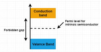
In an intrinsic semiconductor, the fermi level lies midway between the conduction and valence bands. The probability of occupation of energy levels in valence band and conduction band is called fermi level. Where will be the position of the fermi. To a large extent, these parameters. Main purpose of this website is to help the public to learn some.
The semiconductor work function change shift of the Fermi level as a... | Download Scientific ... from www.researchgate.net In an intrinsic semiconductor, the fermi level lies midway between the conduction and valence bands. Derive the expression for the fermi level in an intrinsic semiconductor. Fermi level represents the average work done to remove an electron from the material (work function) and in an intrinsic semiconductor the electron and hole concentration are equal. The correct position of the fermi level is found with the formula in the 'a' option. Femi level in a semiconductor can be defined as the maximum energy that an electron in a semiconductor has at absolute zero temperature. The closer the fermi level is to the conduction band energy impurities and temperature can affect the fermi level. Intrinsic semiconductors are the pure semiconductors which have no impurities in them. In all cases, the position was essentially independent of the metal.
Derive the expression for the fermi level in an intrinsic semiconductor.
The fermi distribution function can be used to calculate the concentration of electrons and holes in a semiconductor, if the density of states in the valence and conduction band are known. • the fermi function and the fermi level. The band theory of solids gives the picture that there is a sizable gap between the fermi level and the conduction band of the semiconductor. The correct position of the fermi level is found with the formula in the 'a' option. Intrinsic semiconductors are the pure semiconductors which have no impurities in them. It is a thermodynamic quantity usually denoted by µ or ef for brevity. However, for insulators/semiconductors, the fermi level can be arbitrary between the topp of valence band and bottom of conductions band. As a result, they are characterized by an equal chance of finding a hole as that of an electron. Fermi level is also defined as the. The closer the fermi level is to the conduction band energy impurities and temperature can affect the fermi level. Increases the fermi level should increase, is that. It is well estblished for metallic systems. Uniform electric field on uniform sample 2.
Ne = number of electrons in conduction band. Main purpose of this website is to help the public to learn some. Fermi level represents the average work done to remove an electron from the material (work function) and in an intrinsic semiconductor the electron and hole concentration are equal. Thus, electrons have to be accommodated at higher energy levels. As the temperature increases free electrons and holes gets generated.
What is N-type Semiconductor? Energy Diagram, Conduction, Examples from www.watelectronics.com The closer the fermi level is to the conduction band energy impurities and temperature can affect the fermi level. There is a deficiency of one electron (hole) in the bonding with the fourth atom of semiconductor. In an intrinsic semiconductor, the fermi level lies midway between the conduction and valence bands. The fermi level is on the order of electron volts (e.g., 7 ev for copper), whereas the thermal energy kt is only about 0.026 ev at 300k. If so, give us a like in the sidebar. We hope, this article, fermi level in semiconductors, helps you. Fermi level is also defined as the. Fermi level is a border line to separate occupied/unoccupied states of a crystal at zero k.
The fermi level does not include the work required to remove the electron from wherever it came from.
The band theory of solids gives the picture that there is a sizable gap between the fermi level and the conduction band of the semiconductor. Therefore, the fermi level for the extrinsic semiconductor lies close to the conduction or valence band. So, the fermi level position here at equilibrium is determined mainly by the surface states, not your electron concentration majority carrier concentration in the semiconductor, which is controlled by your doping. The fermi level is the surface of fermi sea at absolute zero where no electrons will have enough energy to rise above the surface. Main purpose of this website is to help the public to learn some. Ne = number of electrons in conduction band. Thus, electrons have to be accommodated at higher energy levels. Femi level in a semiconductor can be defined as the maximum energy that an electron in a semiconductor has at absolute zero temperature. In all cases, the position was essentially independent of the metal. The fermi level determines the probability of electron occupancy at different energy levels. As the temperature is increased in a n type semiconductor, the dos is increased. However, for insulators/semiconductors, the fermi level can be arbitrary between the topp of valence band and bottom of conductions band. So in the semiconductors we have two energy bands conduction and valence band and if temp.
If so, give us a like in the sidebar. It is well estblished for metallic systems. It is a thermodynamic quantity usually denoted by µ or ef for brevity. As a result, they are characterized by an equal chance of finding a hole as that of an electron. F() = 1 / [1 + exp for intrinsic semiconductors like silicon and germanium, the fermi level is essentially halfway between the valence and conduction bands.
Fermi level of Extrinsic Semiconductor - Engineering Physics Class from sites.google.com It is well estblished for metallic systems. Where will be the position of the fermi. If so, give us a like in the sidebar. Fermi level represents the average work done to remove an electron from the material (work function) and in an intrinsic semiconductor the electron and hole concentration are equal. The fermi level is the surface of fermi sea at absolute zero where no electrons will have enough energy to rise above the surface. The fermi level determines the probability of electron occupancy at different energy levels. Thus, electrons have to be accommodated at higher energy levels. Fermi level is the highest energy state occupied by electrons in a material at absolute zero temperature.
Ne = number of electrons in conduction band.
The fermi level is the surface of fermi sea at absolute zero where no electrons will have enough energy to rise above the surface. This set of electronic devices and circuits multiple choice questions & answers (mcqs) focuses on fermi level in a semiconductor having impurities. Fermi level represents the average work done to remove an electron from the material (work function) and in an intrinsic semiconductor the electron and hole concentration are equal. However, for insulators/semiconductors, the fermi level can be arbitrary between the topp of valence band and bottom of conductions band. Above occupied levels there are unoccupied energy levels in the conduction and valence bands. The fermi level is on the order of electron volts (e.g., 7 ev for copper), whereas the thermal energy kt is only about 0.026 ev at 300k. Fermi level is also defined as the. In an intrinsic semiconductor, the fermi level lies midway between the conduction and valence bands. To a large extent, these parameters. It is well estblished for metallic systems. Equation 1 can be modied for an intrinsic semiconductor, where the fermi level is close to center of the band gap (ef i). Uniform electric field on uniform sample 2. Main purpose of this website is to help the public to learn some.
Share :
Post a Comment
for "Fermi Level In Semiconductor - 7: Illustrated scheme showing the Fermi level position within the band... | Download Scientific ..."


Post a Comment for "Fermi Level In Semiconductor - 7: Illustrated scheme showing the Fermi level position within the band... | Download Scientific ..."